| CPC H10K 59/00 (2023.02) [G09G 3/3233 (2013.01); G09G 3/3258 (2013.01); H01L 27/1255 (2013.01); G09G 2300/043 (2013.01); G09G 2300/0426 (2013.01); G09G 2300/0819 (2013.01); G09G 2300/0842 (2013.01); G09G 2300/0861 (2013.01); G09G 2310/0251 (2013.01); G09G 2310/0262 (2013.01); G09G 2320/043 (2013.01); H10K 59/126 (2023.02); H10K 59/131 (2023.02)] | 20 Claims |
|
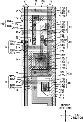
1. A display device comprising:
a first scan line extending in a first direction;
a data line extending in a second direction crossing the first direction;
a first transistor comprising a first semiconductor layer and a first gate electrode, wherein the first semiconductor layer is electrically connected to the data line via a first contact hole;
a second transistor electrically connected to the first transistor, the second transistor comprising a second semiconductor layer and a second gate electrode;
a third transistor comprising a third semiconductor layer and a third gate electrode;
a node connection line, wherein a first portion of the node connection line is electrically connected to the third semiconductor layer via a second contact hole, and a second portion of the node connection line is electrically connected to the second gate electrode via a third contact hole;
a shielding portion, wherein an end portion of the shielding portion disposed between the first contact hole and the second contact hole in a plan view; and
a driving voltage line extending in the second direction, wherein a portion of the driving voltage line overlaps a portion of the third semiconductor layer.
|