| CPC H10K 50/865 (2023.02) [H10K 50/86 (2023.02); H10K 59/122 (2023.02); H10K 59/131 (2023.02); H10K 59/38 (2023.02); H10K 59/40 (2023.02)] | 20 Claims |
|
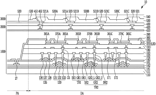
1. A display device comprising:
a substrate;
a plurality of transistors disposed on the substrate;
an insulating layer disposed on the plurality of transistors;
a data line and a driving voltage line disposed on the insulating layer;
a pixel electrode disposed on the data line or the driving voltage line;
a pixel defining layer disposed on the pixel electrode and including a pixel opening that overlaps the pixel electrode;
a light emitting element layer disposed in the pixel opening; and
a common electrode disposed on the light emitting element layer,
wherein the pixel opening comprises a first sub-pixel opening and a second sub-pixel opening, and a first blocking portion that is disposed between the first sub-pixel opening and the second sub-pixel opening, and blocks light.
|