| CPC H10K 50/844 (2023.02) [H01L 29/786 (2013.01); H10K 71/00 (2023.02)] | 19 Claims |
|
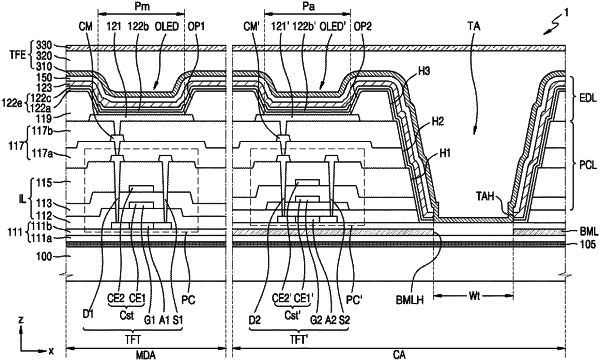
1. A display apparatus comprising a main display area, a component area comprising a transmission area, and a peripheral area located outside the main display area, the display apparatus further comprising:
a first substrate comprising transparent polyimide;
a main display element located on the first substrate to correspond to the main display area;
a main pixel circuit located on the first substrate to correspond to the main display area, comprising a first semiconductor layer connected to the main display element;
an auxiliary display element located on the first substrate to correspond to the component area;
an auxiliary pixel circuit located on the first substrate to correspond to the component area, comprising a second semiconductor layer connected to the auxiliary display element;
a buffer layer located between the first substrate and the first semiconductor layer and between the first substrate and the second semiconductor layer;
a barrier layer located between the first substrate and the buffer layer, comprising one material from among a nitrogen rich silicon nitride (SiNx) having low or no hydrogen content with x being greater than 4/3 and zirconium oxide (Zr2O3), and having a density ranging from about 2 g/cm3 to about 6 g/cm3;
a second substrate located under the first substrate and the second substrate comprising transparent polyimide;
a first inorganic layer located between the first substrate and the second substrate; and
a second inorganic layer directly located on the first inorganic layer.
|