| CPC H10K 50/84 (2023.02) [G06F 3/0412 (2013.01); G06F 3/0443 (2019.05); G06F 3/0446 (2019.05); H10K 59/131 (2023.02); H10K 59/40 (2023.02); H10K 59/65 (2023.02); H10K 77/111 (2023.02); G06F 3/044 (2013.01); G06F 2203/04111 (2013.01); G09G 3/3233 (2013.01); G09G 2320/0233 (2013.01); H10K 2102/311 (2023.02)] | 8 Claims |
|
1. An electroluminescent device, comprising:
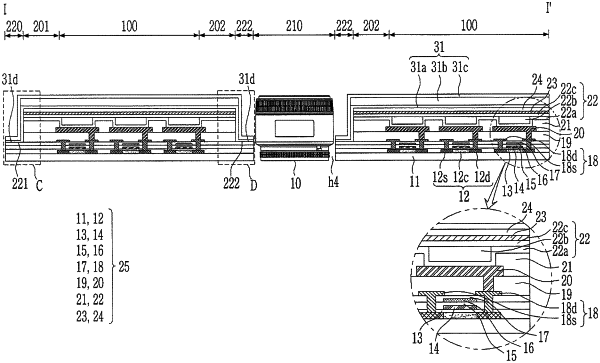
a lower structure comprising a light transmitting region, a non-transparent emission area surrounding the light transmitting region in a plan view and having a light transmittance lower than the light transmitting region, and an outer non-emission area surrounding the non-transparent emission area in a plan view, and
an encapsulation structure located on the lower structure and having an inorganic lower surface,
wherein the outer non-emission area has an outer inorganic surface portion surrounding the non-transparent emission area in a plan view and making a direct contact with the inorganic lower surface to form an inorganic-inorganic contact region surrounding the non-transparent emission area in a plan view,
the lower structure comprises:
an inorganic structure comprising a buffer layer including an inorganic material and a transistor on the buffer layer;
a planarization layer located on the inorganic structure;
a lower electrode located on the planarization layer;
a pixel defining layer located on the planarization layer to cover a side portion of the lower electrode;
an intermediate multilayer located on the lower electrode and having at least one functional layer; and
an upper electrode located on the intermediate multilayer, and
the light transmitting region corresponds a through hole,
the lower structure comprises an inner buffer area located between the non-transparent emission area and the light transmitting region to surround the light transmitting region in a plan view,
the lower structure comprises a current wire overlapping the non-transparent emission area and an inner bus wire electrically connected to the current wire and located in the inner buffer area in a plan view, and
the inner bus wire includes first parts extending in a first direction and second parts extending in a second direction different from the first direction, and
the inner bus wire completely surrounds the light transmitting region in a plan view.
|