| CPC H10K 59/124 (2023.02) [H10K 59/1216 (2023.02); H10K 59/131 (2023.02); H10K 77/111 (2023.02); H01L 27/124 (2013.01); H01L 27/1218 (2013.01); H01L 27/1248 (2013.01); H10K 59/1201 (2023.02); H10K 2102/311 (2023.02); Y02E 10/549 (2013.01)] | 18 Claims |
|
1. A display device having a bendable region and a non-bendable region arranged in a first direction, the display device comprising:
a substrate disposed in the bendable region and the non-bendable region;
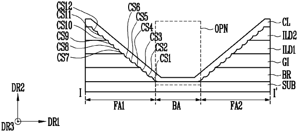
a barrier layer disposed on the substrate in the non-bendable region and having a first side surface adjacent to the bendable region;
an active pattern disposed on the barrier layer;
a first insulating layer disposed on the barrier layer and the active pattern and having a second side surface adjacent to the bendable region, the second side surface being farther from the bendable region in the first direction than the first side surface;
a first conductive pattern overlapping the active pattern and disposed on the first insulating layer;
a second insulating layer disposed on the first conductive pattern and the first insulating layer and having a third side surface adjacent to the bendable region, the third side surface being farther from the bendable region in the first direction than the second side surface;
a second conductive pattern disposed on the second insulating layer;
a third insulating layer disposed on the second conductive pattern and the second insulating layer and having a fourth side surface adjacent to the bendable region, the fourth side surface being farther from the bendable region in the first direction than the third side surface;
a third conductive pattern disposed on the third insulating layer; and
a conductive layer contacting the first to fourth side surfaces and extending to the bendable region, the conductive layer contacting the substrate in the bendable region.
|