| CPC H10B 63/84 (2023.02) [G11C 13/004 (2013.01); G11C 13/0004 (2013.01); G11C 13/0069 (2013.01); H10N 70/231 (2023.02); G11C 2213/71 (2013.01)] | 16 Claims |
|
1. A semiconductor device, comprising:
first row lines each extending in a first direction;
column lines each extending in a second direction crossing the first direction;
second row lines each extending in the first direction;
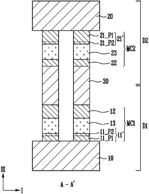
a plurality of first memory cells respectively coupled between the first row lines and the column lines, each of the plurality of first memory cells including a first variable resistance layer and a first electrode positioned between the first variable resistance layer and a corresponding one of the first row lines; and
a plurality of second memory cells respectively coupled between the second row lines and the column lines, each of the plurality of second memory cells including a second variable resistance layer and a second electrode positioned between the second variable resistance layer and a corresponding one of the second row lines,
wherein the first electrode, or the second electrode, or both include a first portion and a second portion, the second portion having a nitrogen concentration higher than that of the first portion and being disposed between the first portion and a corresponding one of the first and second variable resistance layers.
|