| CPC H10B 43/40 (2023.02) [G11C 16/08 (2013.01); G11C 16/24 (2013.01); G11C 16/30 (2013.01); H10B 43/20 (2023.02); H10B 43/35 (2023.02)] | 13 Claims |
|
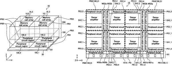
1. A semiconductor memory device comprising:
a memory cell array provided above a substrate in a first direction and including a plurality of memory cells, the first direction intersecting a surface of the substrate;
a first peripheral circuit provided between the substrate and the memory cell array;
a second peripheral circuit provided between the substrate and the memory cell array and apart from the first peripheral circuit in a second direction, the second direction being parallel to the surface of the substrate; and
a sense amplifier provided between the substrate and the memory cell array and between the first peripheral circuit and the second peripheral circuit,
wherein a length of the second peripheral circuit in the second direction is smaller than half of a length of the sense amplifier in the second direction.
|