| CPC H10B 43/30 (2023.02) [H10B 41/30 (2023.02)] | 18 Claims |
|
1. A semiconductor memory device comprising:
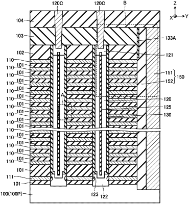
a substrate;
a plurality of first conductive layers and a plurality of first insulating layers stacked in alternation in a first direction intersecting with a surface of the substrate;
a first semiconductor layer that extends in the first direction and is opposed to the plurality of first conductive layers and the plurality of first insulating layers;
a second semiconductor layer that is connected to one end portion in the first direction of the first semiconductor layer and extends in a second direction intersecting with the first direction;
a second insulating layer that covers an outer peripheral surface of another end portion of the first semiconductor layer; and
a third insulating layer disposed at a position in the second direction different from the plurality of first conductive layers, the plurality of first insulating layers, and the second insulating layer, the third insulating layer extending in the first direction, the third insulating layer having one end in the first direction in contact with the second semiconductor, the third insulating layer having another end in the first direction farther from the second semiconductor layer than the second insulating layer, wherein
a metal oxide film is disposed on a surface on the third insulating layer side in the second direction of the second insulating layer, and
a metal oxide film is absent on a surface on the third insulating layer side in the second direction of the plurality of first insulating layers.
|