| CPC H10B 43/27 (2023.02) [H10B 41/10 (2023.02); H10B 41/27 (2023.02); H10B 41/35 (2023.02); H10B 41/41 (2023.02); H10B 43/10 (2023.02); H10B 43/35 (2023.02); H10B 43/40 (2023.02)] | 20 Claims |
|
1. A three-dimensional semiconductor memory device, comprising:
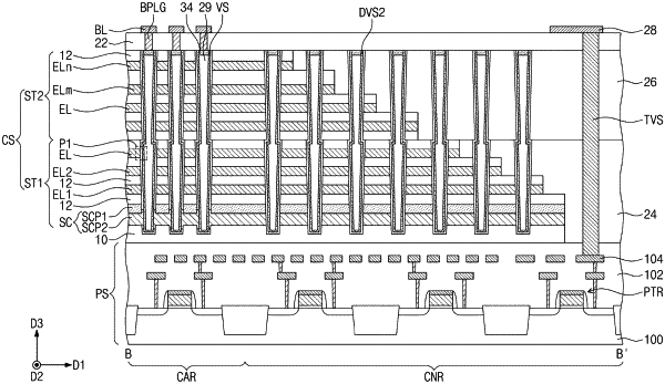
a peripheral logic structure, the peripheral logic structure including a first substrate, a peripheral transistor on the first substrate, and a peripheral connection line electrically connected to the peripheral transistor; and
a cell array structure on the peripheral logic structure and electrically connected to the peripheral logic structure,
wherein the cell array structure comprises:
a second substrate on the peripheral logic structure;
a stack on the second substrate, the stack including a plurality of intergate dielectric layers and a plurality of electrode layers that are alternately stacked on the second substrate;
a vertical semiconductor pattern that penetrates the stack and extends into the second substrate; and
a vertical insulating pattern between the stack and the vertical semiconductor pattern,
wherein the plurality of intergate dielectric layers includes a first intergate dielectric layer and a second intergate dielectric layer that are vertically adjacent to each other,
wherein the plurality of electrode layers include a first electrode layer interposed between the first and second intergate dielectric layers,
wherein the vertical insulating pattern includes a blocking dielectric pattern, a charge storage pattern, and a tunnel dielectric layer that are sequentially interposed between the first electrode layer and the vertical semiconductor pattern,
wherein the tunnel dielectric layer extends from a first sidewall of the first intergate dielectric layer through the charge storage pattern to a second sidewall of the second intergate dielectric layer,
wherein the tunnel dielectric layer is in direct contact with the first sidewall of the first intergate dielectric layer and the second sidewall of the second intergate dielectric layer, and
wherein both the tunnel dielectric layer and the charge storage pattern are in direct contact with each of the first intergate dielectric layer and the second intergate dielectric layer.
|