| CPC H10B 43/27 (2023.02) [H10B 43/10 (2023.02)] | 20 Claims |
|
1. A method for fabricating a nonvolatile memory device, the method comprising:
forming a first sacrificial pattern and an insulating pattern alternately stacked on a substrate;
forming a second sacrificial pattern on the first sacrificial pattern and the insulating pattern;
forming a first cutting line which cuts the second sacrificial pattern;
forming a third sacrificial pattern on the second sacrificial pattern and the first cutting line;
forming a second cutting line which is spaced apart from the first cutting line, as viewed from a planar view, and cuts the third sacrificial pattern;
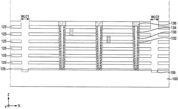
forming first and second word line cutting regions which penetrate the first to third sacrificial patterns and the insulating pattern, and are spaced apart from each other with the second sacrificial pattern and the third sacrificial pattern interposed therebetween; and
replacing the first to third sacrificial patterns with a plurality of conductive patterns, using the first and second word line cutting regions.
|