| CPC H10B 43/27 (2023.02) [H01L 29/7926 (2013.01); H10B 41/27 (2023.02); H10B 41/40 (2023.02); H10B 41/50 (2023.02); H10B 43/50 (2023.02); H10B 43/40 (2023.02)] | 20 Claims |
|
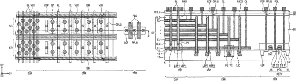
1. A three-dimensional semiconductor memory device, comprising:
a substrate including a cell array region and a connection region;
an electrode structure including a plurality of electrodes vertically stacked on the substrate;
a plurality of first vertical channels that penetrate the electrode structure on the cell array region;
a plurality of second vertical channels that penetrate the electrode structure on the connection region;
a dummy insulating pattern provided in the connection region of the substrate,
wherein each of the first vertical channels and the second vertical channels includes a lower channel pattern connected to the substrate and an upper channel pattern connected to the lower channel pattern,
wherein a lowermost electrode of the plurality of electrodes surrounds the lower channel patterns of the first vertical channels and the upper channel patterns of the second vertical channels,
wherein top-most surfaces of the lower channel patterns of the second vertical channels are positioned at a lower level than a top surface of the substrate,
wherein the dummy insulating pattern is spaced apart from the plurality of first vertical channels, and
wherein the dummy insulating pattern contacts sidewalls of the lower channel patterns of the second vertical channels.
|
|
12. A three-dimensional semiconductor memory device, comprising:
a substrate including a cell array region and a connection region;
an electrode structure including a plurality of electrodes stacked in a first direction perpendicular to a top surface of the substrate, the electrode structure having a staircase-shape on the connection region;
a first vertical channel that penetrates the electrode structure on the cell array region, the first vertical channel including a first lower channel pattern in direct contact with the substrate and a first upper channel pattern connected to the first lower channel pattern; and
a second vertical channel that penetrates the electrode structure on the connection region, the second vertical channel including a second lower channel pattern in direct contact with the substrate and a second upper channel pattern connected to the second low pattern,
wherein a lowermost electrode of the plurality of electrodes surrounds the first lower channel pattern and the second upper channel pattern,
wherein a sidewall of the second lower channel pattern is spaced apart from the substrate,
wherein a top surface of the second lower channel pattern is positioned at a lower level than a bottom surface of the lowermost electrode, and
wherein each of the first lower channel pattern and the second lower channel pattern comprises a pillar-shaped epitaxial pattern directly contacting the substrate.
|
|
20. A three-dimensional semiconductor memory device, comprising:
a substrate including a cell array region and a connection region;
an electrode structure including a plurality of electrodes vertically stacked on the substrate;
a plurality of first vertical channels that penetrate the electrode structure on the cell array region; and
a plurality of second vertical channels that penetrate the electrode structure on the connection region,
wherein each of the plurality of first vertical channels and each of the plurality of second vertical channels includes a lower channel pattern in direct contact with the substrate and an upper channel pattern connected to the lower channel pattern and a sidewall of the second lower channel pattern is spaced apart from the substrate,
wherein a lowermost electrode of the plurality of electrodes surrounds the lower channel pattern of each of the plurality of first vertical channels and the upper channel pattern of each of the plurality of second vertical channels,
wherein top surfaces of the lower channel pattern of each of the plurality of second vertical channels are positioned at a lower level than a bottom surface of the lowermost electrode,
wherein the top surfaces of each of the plurality of lower channel patterns of the second vertical channels are positioned at a lower level than a top surface of the substrate, and
wherein each of the lower channel patterns of the first and second vertical channels comprises a pillar-shaped epitaxial pattern directly contacting the substrate.
|