| CPC H10B 12/488 (2023.02) [H01L 21/76224 (2013.01); H01L 23/53271 (2013.01); H01L 29/0607 (2013.01); H01L 29/78 (2013.01); H10B 12/053 (2023.02); H10B 12/34 (2023.02)] | 8 Claims |
|
1. A method for manufacturing a semiconductor device, comprising following steps:
providing a semiconductor substrate, and forming active regions and trench isolation structures in the semiconductor substrate, wherein the trench isolation structures are located between the active regions;
forming first grooves in the active regions;
filling the first grooves to form inversion polysilicon layers, the inversion polysilicon layers being inversely doped with the active regions;
forming second grooves, the second grooves running through the inversion polysilicon layers and a part of the semiconductor substrate, and reserving parts of the inversion polysilicon layers located on side faces of the second grooves; and
forming buried word line structures in the second grooves;
wherein, the step of forming the buried word line structures further comprises:
forming gate oxide layers on surfaces of the second grooves;
forming gate block layers on surfaces of the gate oxide layers, the gate block layers covering bottom surfaces and parts of side faces of the gate oxide layers;
forming gate conductive layers on surfaces of the gate block layers, the gate conductive layers filling parts of the second grooves; and
forming insulating filling layers on the gate block layers and the gate conductive layers, the insulating filling layers filling remaining parts of the second grooves;
wherein, the steps of forming the gate block layers and forming the gate conductive layers comprise:
forming primary block layers on surfaces of the gate oxide layers;
forming primary conductive layers on surfaces of the primary block layers and filling the second grooves; and
removing parts of the primary conductive layers and parts of the primary block layers, reserving second parts of the primary conductive layers and second parts of the primary block layers located in bottom regions of the second grooves to form the gate block layers and the gate conductive layers, a height of the parts of the primary conductive layers that are removed and the parts of the primary block layers that are removed is 20 nm to 150 nm.
|
|
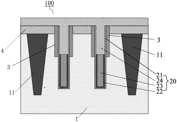
6. A semiconductor device, comprising:
a semiconductor substrate, having active regions and trench isolation structures located between the active regions;
buried word line structures, located in the active regions, the buried word line structures comprise: gate oxide layers, gate block layers, gate conductive layers and insulating filling layers, the gate block layers being located on surfaces of the gate conductive layers, the insulating filling layers being located on the gate conductive layers and the gate block layers, and the gate oxide layers being located on surfaces of both the gate block layers and the insulating filling layers; and
inversion polysilicon layers, located on side faces of the buried word line structures and inversely doped with the active regions, upper surfaces of the inversion polysilicon layers are flush with upper surfaces of the gate oxide layers, a thickness of each of the inversion polysilicon layers is 5 nm to 25 nm, and a height of each of the inversion polysilicon layers is 20 nm to 150 nm.
|