| CPC H10B 12/30 (2023.02) [H10B 12/03 (2023.02); H10B 12/05 (2023.02); H10B 12/482 (2023.02); H10B 12/488 (2023.02); H10B 12/50 (2023.02); H01L 29/7869 (2013.01); H01L 29/78672 (2013.01); H01L 29/78684 (2013.01)] | 27 Claims |
|
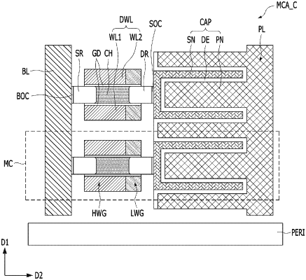
1. A semiconductor memory device comprising:
an active layer spaced apart from a substrate wherein the active layer extends in a direction parallel to the substrate and includes a channel;
a bit line extending in a direction perpendicular to the substrate and coupled to a first end of the active layer;
a capacitor coupled to an end of a second end of the active layer;
a double word line including a pair of dual work function electrodes extending in a direction crossing the active layer with the active layer interposed therebetween; and
a gate dielectric layer formed between the active layer and the double word line,
wherein each of the dual work function electrodes includes:
a high work function electrode which is adjacent to the bit line; and
a low work function electrode which is adjacent to the capacitor and having a lower work function than the high work function electrode,
wherein the high work function electrode is in direct contact with the low work function electrode.
|