| CPC H10B 12/033 (2023.02) [H01L 21/28238 (2013.01); H01L 28/91 (2013.01); H01L 28/92 (2013.01); H10B 12/315 (2023.02); H10B 12/318 (2023.02)] | 23 Claims |
|
1. A method of fabricating a semiconductor device, the method comprising:
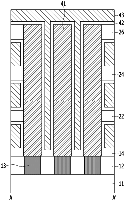
sequentially forming a substructure over a substrate and a etch stop layer over the substructure;
forming a stack structure of alternately stacked mold layers and supporter layers over the etch stop layer;
forming a plurality of supporter holes in the stack structure exposing the etch stop layer;
forming a sacrificial layer filling each of the plurality of the supporter holes;
forming a plurality of lower electrode openings exposing the substructure by etching the sacrificial layer and the stack structure; and
forming a lower electrode inside the plurality of lower electrode openings.
|