| CPC H05K 1/115 (2013.01) [H01L 21/486 (2013.01); H01L 21/4846 (2013.01); H01L 23/481 (2013.01); H01L 23/49822 (2013.01); H01L 33/62 (2013.01); H05K 1/095 (2013.01); H05K 3/0094 (2013.01); H05K 3/4038 (2013.01); H05K 3/4069 (2013.01); H01L 2933/0066 (2013.01); H05K 1/112 (2013.01); H05K 2201/09454 (2013.01); H05K 2201/09572 (2013.01); H05K 2201/09854 (2013.01); H05K 2201/10106 (2013.01); H05K 2203/0126 (2013.01); H05K 2203/0139 (2013.01); H05K 2203/0278 (2013.01); H05K 2203/1105 (2013.01)] | 15 Claims |
|
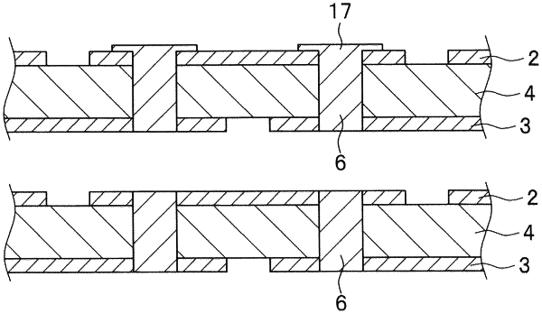
1. A method of manufacturing a circuit substrate, the method comprising:
forming, in an insulating substrate and circuit patterns that are provided on a first surface and a second surface of the insulating substrate, a through-hole penetrating the insulating substrate and the circuit patterns such that the through-hole extends from a first hole opening to a second hole opening, the circuit patterns contain Cu as a main component;
filling, in the through-hole, an electrically conductive paste that is a melting-point shift electrically conductive paste including Sn—Bi solder powder, Cu powder, and resin, and forming a protrusion obtained by causing the electrically conductive paste to protrude from the through-hole;
performing pressure treatment on the protrusion near the through-hole; and
performing heat treatment on the insulating substrate whose protrusion is subjected to the pressure treatment and causing the circuit patterns and the electrically conductive paste to be electrically connected with each other,
in the performing pressure treatment, a diameter of the through-hole at a center in a thickness direction of the insulating substrate is larger than diameters of the first hole opening and the second hole opening.
|