| CPC H05K 1/0296 (2013.01) [H05K 3/18 (2013.01); H05K 2201/09227 (2013.01); H05K 2203/0723 (2013.01)] | 4 Claims |
|
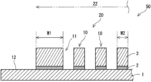
1. A printed circuit board comprising:
an insulating base film, and
a plurality of wiring portions formed on a surface of the base film,
wherein the wiring portions include a seed layer that is directly or indirectly layered on the surface of the base film and a metal layer that is layered on the seed layer,
wherein the base film has a wiring area including the plurality of wiring portions and a non-wiring area not including the wiring portions,
wherein the plurality of wiring portions include at least one outermost boundary wiring portion and a plurality of inner wiring portions other than the outermost boundary wiring portion,
wherein the outermost boundary wiring portion is formed on an outermost side of the base film in the wiring area and at a boundary between the wiring area and the non-wiring area,
wherein an average width of the outermost boundary wiring portion is 30 μm or more,
wherein an average width of the inner wiring portions is 20 μm or less, and
wherein an average aspect ratio of the inner wiring portions is 1.5 or more, the average aspect ratio of the inner wiring portions being determined based on a maximum length of a cross section in a thickness direction perpendicular to a longitudinal direction of the inner wiring portions divided by the average width of the inner wiring portions.
|