| CPC H05K 1/0237 (2013.01) [H01Q 1/243 (2013.01); H01Q 5/328 (2015.01); H01Q 13/02 (2013.01); H05K 1/115 (2013.01); H05K 2201/10098 (2013.01)] | 15 Claims |
|
1. An electronic device comprising:
a housing including a first plate, a second plate facing away from the first plate, and a side member surrounding a space between the first plate and the second plate, connected with the second plate or integrally formed with the second plate, and including a conductive material,
wherein a first portion of the side member includes:
a first surface facing an exterior of the housing;
a second surface facing an interior of the housing;
a through hole formed in a first direction being a direction passing through the side member from the first surface to the second surface; and
a non-conductive material inserted into the through hole;
a display viewable through at least a portion of the first plate;
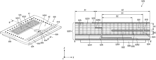
a printed circuit board disposed in the interior of the housing, wherein the printed circuit board includes:
a third surface facing the second surface;
a fourth surface facing away from the third surface;
a first conductive layer disposed closer to the third surface than to the fourth surface and including a slit formed to face the through hole;
a second conductive layer disposed closer to the fourth surface than to the first conductive layer;
a feeding line interposed between the first conductive layer and the second conductive layer;
a conductive pattern interposed between the feeding line and the first conductive layer and electrically coupled with the first conductive layer;
a conductive via connecting the feeding line and the conductive pattern;
a third conductive layer interposed between the first conductive layer and the second conductive layer;
a fourth conductive layer interposed between the first conductive layer and the third conductive layer;
a plurality of first side vias electrically connecting the first conductive layer and the third conductive layer and formed to be spaced from the conductive via in a second direction, which is perpendicular to the first direction and is a direction facing away from the through hole and the slit, as much as a first distance; and
a plurality of second side vias electrically connecting the third conductive layer and the fourth conductive layer and formed to be spaced from the conductive via in the second direction as much as a second distance different from the first distance; and
a wireless communication circuit electrically connected with the feeding line, and configured to transmit and/or receive signals each having a frequency between 3 GHz and 100 GHz.
|