| CPC H05K 1/0218 (2013.01) [H05K 1/024 (2013.01); H05K 1/0256 (2013.01); H05K 1/0298 (2013.01); H05K 2201/0141 (2013.01)] | 21 Claims |
|
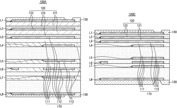
1. A printed circuit board comprising:
a first substrate portion including a plurality of first insulating layers, a plurality of first wiring layers respectively disposed on the plurality of first insulating layers, and a plurality of first adhesive layers respectively disposed between the plurality of first insulating layers to respectively cover the plurality of first wiring layers; and
a second substrate portion disposed on the first substrate portion, and including a plurality of second insulating layers, a plurality of second wiring layers respectively disposed on the plurality of second insulating layers, and a plurality of second adhesive layers respectively disposed between the plurality of second insulating layers to respectively cover the plurality of second wiring layers,
wherein a dissipation factor of each adhesive layer of the plurality of first adhesive layers is lower than a dissipation factor of each adhesive layer of the plurality of second adhesive layers,
the plurality of first wiring layers excluding a lowermost wiring layer are respectively embedded in the plurality of first adhesive layers such that side surfaces of the plurality of first wiring layers excluding the lowermost wiring layer are respectively covered by the plurality of first adhesive layers, and
one of the plurality of second wiring layers is embedded in one of the plurality of second adhesive layers such that side surfaces of the one of the plurality of second wiring layers are covered by the one of the plurality of second adhesive layers.
|