US 11,864,295 B2
Selectively shielded radio frequency module with multi-mode stacked power amplifier stage
Yasser Khairat Soliman, Kanata (CA); Hoang Mong Nguyen, Fountain Valley, CA (US); Anthony James LoBianco, Irvine, CA (US); Gregory Edward Babcock, Ottawa (CA); Darren Roger Frenette, Pakenham (CA); George Khoury, Ottawa (CA); René Rodríguez, Rancho Santa Margarita, CA (US); and Leslie Paul Wallis, Ottawa (CA)
Assigned to Skyworks Solutions, Inc., Irvine, CA (US)
Filed by SKYWORKS SOLUTIONS, INC., Irvine, CA (US)
Filed on Mar. 29, 2021, as Appl. No. 17/216,302.
Application 17/216,302 is a division of application No. 16/820,401, filed on Mar. 16, 2020, granted, now 11,037,893.
Application 16/820,401 is a division of application No. 16/354,923, filed on Mar. 15, 2019, granted, now 10,629,553, issued on Apr. 21, 2020.
Application 16/354,923 is a division of application No. 15/857,217, filed on Dec. 28, 2017, granted, now 10,276,521, issued on Apr. 30, 2019.
Claims priority of provisional application 62/595,935, filed on Dec. 7, 2017.
Claims priority of provisional application 62/594,179, filed on Dec. 4, 2017.
Claims priority of provisional application 62/571,409, filed on Oct. 12, 2017.
Claims priority of provisional application 62/570,459, filed on Oct. 10, 2017.
Claims priority of provisional application 62/480,002, filed on Mar. 31, 2017.
Claims priority of provisional application 62/440,241, filed on Dec. 29, 2016.
Prior Publication US 2021/0217714 A1, Jul. 15, 2021
Int. Cl. H01L 23/66 (2006.01); H05B 47/19 (2020.01); H03F 3/24 (2006.01); H03F 1/32 (2006.01); H01L 23/552 (2006.01); H04B 1/40 (2015.01); H03F 3/195 (2006.01); H03F 1/22 (2006.01); H03F 1/34 (2006.01); H03F 1/56 (2006.01); H04B 1/04 (2006.01); F21V 23/00 (2015.01); H04W 84/12 (2009.01); H01Q 1/38 (2006.01); H01Q 1/22 (2006.01); H01Q 9/42 (2006.01)
CPC H05B 47/19 (2020.01) [F21V 23/006 (2013.01); H01L 23/552 (2013.01); H01L 23/66 (2013.01); H03F 1/223 (2013.01); H03F 1/32 (2013.01); H03F 1/3205 (2013.01); H03F 1/347 (2013.01); H03F 1/565 (2013.01); H03F 3/195 (2013.01); H03F 3/245 (2013.01); H04B 1/0475 (2013.01); H04B 1/40 (2013.01); H01L 2223/665 (2013.01); H01L 2223/6655 (2013.01); H01L 2223/6677 (2013.01); H01L 2224/16145 (2013.01); H01L 2224/16225 (2013.01); H01L 2224/32145 (2013.01); H01L 2224/48091 (2013.01); H01L 2224/48195 (2013.01); H01L 2224/48227 (2013.01); H01L 2224/49171 (2013.01); H01L 2224/73265 (2013.01); H01L 2924/19104 (2013.01); H01Q 1/2283 (2013.01); H01Q 1/38 (2013.01); H01Q 9/42 (2013.01); H03F 2200/222 (2013.01); H03F 2200/294 (2013.01); H03F 2200/451 (2013.01); H03F 2200/534 (2013.01); H04B 2001/0433 (2013.01); H04W 84/12 (2013.01)] 20 Claims
OG exemplary drawing
 
1. A packaged module comprising:
a package substrate;
a radio frequency shielding structure extending above the package substrate;
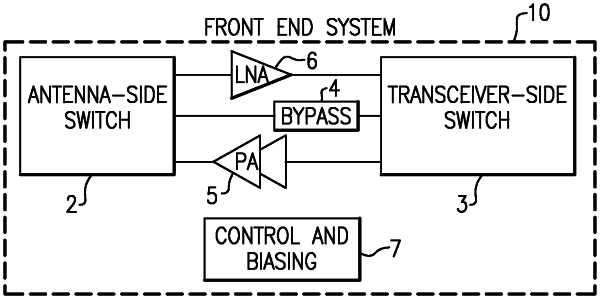
a front end integrated circuit positioned in an interior of the radio frequency shielding structure, the front end integrated circuit including a multi-mode power amplifier circuit that includes an input stage and a stacked output stage that is coupled to the input stage by way of an inter-stage matching network, the stacked output stage including a transistor stack of two or more transistors arranged in series with each other, and a bias circuit configured to bias the transistor stack such that the stacked output stage functions like there is at least one less transistor in the transistor stack in a second mode relative to a first mode; and
an antenna on the package substrate external to the radio frequency shielding structure.