US 11,863,898 B2
Solid state imaging device and electronic apparatus
Shoji Kobayashi, Kanagawa (JP); Yoshiharu Kudoh, Kanagawa (JP); and Takuya Sano, Kanagawa (JP)
Assigned to Sony Group Corporation, Tokyo (JP)
Filed by Sony Group Corporation, Tokyo (JP)
Filed on Nov. 8, 2021, as Appl. No. 17/521,649.
Application 17/521,649 is a continuation of application No. 16/748,564, filed on Jan. 21, 2020, granted, now 11,183,529.
Application 16/748,564 is a continuation of application No. 16/188,876, filed on Nov. 13, 2018, granted, now 10,580,815, issued on Mar. 3, 2020.
Application 16/188,876 is a continuation of application No. 15/487,283, filed on Apr. 13, 2017, granted, now 10,163,950, issued on Dec. 25, 2018.
Application 15/487,283 is a continuation of application No. 15/412,811, filed on Jan. 23, 2017, granted, now 9,899,440, issued on Feb. 20, 2018.
Application 15/412,811 is a continuation of application No. 15/087,709, filed on Mar. 31, 2016, granted, now 9,647,024, issued on May 9, 2017.
Application 15/087,709 is a continuation of application No. 14/881,818, filed on Oct. 13, 2015, granted, now 9,613,997, issued on Apr. 4, 2017.
Application 14/881,818 is a continuation of application No. 14/057,542, filed on Oct. 18, 2013, granted, now 9,197,829, issued on Nov. 24, 2015.
Application 14/057,542 is a continuation of application No. 13/227,851, filed on Sep. 8, 2011, granted, now 8,587,040, issued on Nov. 19, 2013.
Claims priority of application No. 2010-206890 (JP), filed on Sep. 15, 2010.
Prior Publication US 2022/0141410 A1, May 5, 2022
Int. Cl. H04N 25/76 (2023.01); H01L 27/146 (2006.01); H04N 23/55 (2023.01); H04N 23/54 (2023.01); H04N 25/70 (2023.01)
CPC H04N 25/76 (2023.01) [H01L 27/1462 (2013.01); H01L 27/1464 (2013.01); H01L 27/14603 (2013.01); H01L 27/14605 (2013.01); H01L 27/14612 (2013.01); H01L 27/14621 (2013.01); H01L 27/14623 (2013.01); H01L 27/14625 (2013.01); H01L 27/14627 (2013.01); H01L 27/14629 (2013.01); H01L 27/14636 (2013.01); H01L 27/14643 (2013.01); H01L 27/14645 (2013.01); H04N 23/54 (2023.01); H04N 23/55 (2023.01); H04N 25/70 (2023.01); H01L 27/14609 (2013.01)] 12 Claims
OG exemplary drawing
 
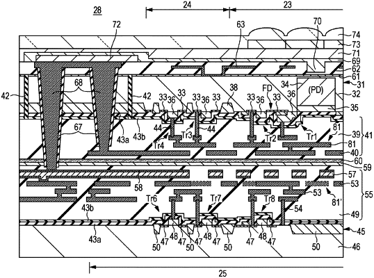
1. A light detecting device, comprising:
a pixel region that is formed on a light incident side of a first substrate and in which a plurality of pixels that include photoelectric conversion units is arranged;
a circuit unit that is formed in a second substrate below at least one of the plurality of pixels in the first substrate;
a first multilayer-wiring layer that includes a first wiring layer having a first wiring and a second wiring layer having a second wiring; and
a second multilayer-wiring layer formed at a side of the second substrate, wherein the second multilayer-wiring layer includes a third wiring layer having a third wiring and a fourth wiring layer having a fourth wiring, and wherein the first substrate and the second substrate are stacked;
wherein,
the first multilayer-wiring layer and the second multilayer-wiring layer are disposed between the pixel region and the circuit unit, and
one of the first wiring, the second wiring, the third wiring or the fourth wiring, extending in a first direction, at least partially overlaps with another of the first wiring, the second wiring, the third wiring or the fourth wiring extending in the first direction.