| CPC H04N 23/54 (2023.01) [H04N 23/51 (2023.01); H04N 23/52 (2023.01); H04N 23/57 (2023.01); H05K 1/181 (2013.01); H05K 2201/10151 (2013.01)] | 9 Claims |
|
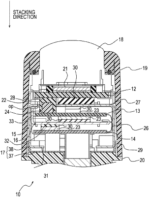
1. An electronic device comprising:
a first substrate, a second substrate, and a third substrate on each of which an electronic component is mounted, the first substrate, the second substrate, and the third substrate being positioned in order toward a stacking direction with respective main surfaces facing each other;
a first metal plate including
a first flat portion that is interposed between the first substrate and the second substrate and that directly or indirectly abuts the electronic component mounted on the first substrate and the electronic component mounted on the second substrate, and
a first shield portion that covers an entire circumference of a side surface of the first substrate; and
a second metal plate including
a second flat portion that is interposed between the second substrate and the third substrate and that directly or indirectly abuts the electronic component mounted on the second substrate and the electronic component mounted on the third substrate, and
a second shield portion that covers at least portions of side surfaces of the second substrate and the third substrate.
|