| CPC H03M 1/785 (2013.01) [H03M 1/747 (2013.01); H03K 17/60 (2013.01); H03M 1/0658 (2013.01); H03M 1/66 (2013.01); H03M 1/78 (2013.01)] | 16 Claims |

|
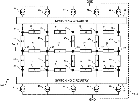
1. Differential circuitry comprising:
first and second current paths each comprising a succession of first and further load nodes, each successive further load node connected to its preceding load node via a divider impedance; and
first switching circuitry connected to the further load node or nodes of the first current path, and second switching circuitry connected to the further load node or nodes of the second current path, the first and second switching circuitry configured to control a magnitude of controllable current signals passing through the load nodes of the first current path and the second current path, respectively,
wherein:
the first load nodes of the first and second current paths comprise a first pair of load nodes, and the or each successive further load node of the first current path and its corresponding successive further load node of the second current path comprise a successive further pair of load nodes;
the first pair of load nodes are connected to a first common node via respective first load impedances and the or each successive further pair of load nodes are connected to a successive further common node via respective further load impedances;
the or each successive further common node is connected to its preceding common node; and
the or at least one of the successive further common nodes is connected to its preceding common node via a resistor.
|