| CPC H03M 1/0626 (2013.01) [H03M 1/1245 (2013.01); H03M 1/462 (2013.01); H03M 1/464 (2013.01); H03M 1/84 (2013.01); H03M 3/32 (2013.01); H03M 3/43 (2013.01); H03M 3/462 (2013.01); H03M 3/476 (2013.01)] | 20 Claims |
|
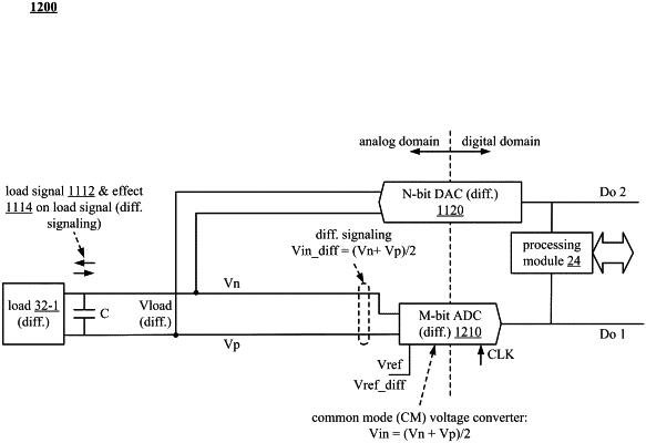
1. An analog to digital converter (ADC) comprising:
a capacitor operably coupled to a first node and a second node of a differential load and configured to produce a differential load voltage based on charging by a differential load current and a differential digital to analog converter (DAC) output current, wherein the ADC is coupled to the first node and the second node of the differential load;
a common mode analog circuit operably coupled to the first node and the second node of the differential load, wherein, when enabled, the common mode analog circuit is configured to convert a differential signal at the first node and the second node of the differential load to a single-ended load voltage;
a differential M-bit analog to digital converter (ADC) operably coupled to the differential load, wherein, when enabled, the M-bit ADC configured to:
receive the differential load voltage;
receive a differential reference voltage; and
compare the differential load voltage to the differential reference voltage and generate a first digital output signal that is representative of a difference between the differential load voltage and the differential reference voltage;
memory that stores operational instructions;
one or more processing modules operably coupled to the differential M-bit ADC and the memory, wherein, when enabled, the one or more processing modules configured to execute the operational instructions to process the first digital output signal to generate a second digital output signal that is representative of the difference between the differential load voltage and the differential reference voltage, wherein the second digital output signal includes a higher resolution than the first digital output signal; and
an N-bit digital to analog converter (DAC) that is operably coupled to the one or more processing modules, wherein, when enabled, the N-bit DAC configured to generate the differential DAC output current based on the second digital output signal, the differential DAC output current tracks the differential load current, and the differential load voltage tracks the differential reference voltage, wherein:
N is a first positive integer;
M is a second positive integer greater than or equal to 1; and
N is greater than M.
|