| CPC H03K 3/0372 (2013.01) [H03K 19/20 (2013.01)] | 18 Claims |
|
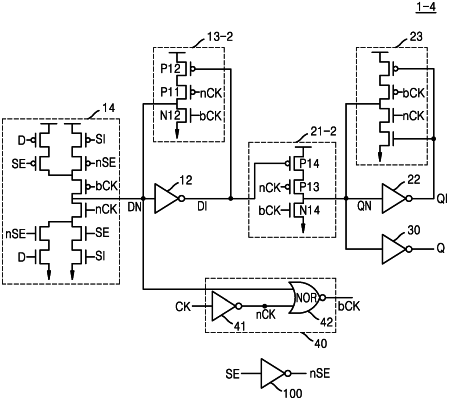
1. A flip-flop circuit comprising:
a first master latch circuit configured to transmit a first inverted signal of a first input signal received from an external device to a first node and transmit a second inverted signal of the first inverted signal at the first node to a second node, based on a first control signal having a first logic level or a second control signal having a second logic level;
a first slave latch circuit configured to transmit a third inverted signal of the second inverted signal at the second node to a third node according to the first control signal having the second logic level or the second control signal having the first logic level;
a first output inverter configured to generate a first output signal by inverting the third inverted signal at the third node; and
a first control signal generation circuit configured to generate the first control signal and the second control signal based on a clock signal and the first inverted signal at the first node,
wherein the first slave latch circuit comprises a first tri-state inverter configured to transmit the second inverted signal of the second node to the third node based on the first control signal and the second control signal, and
wherein the first tri-state inverter comprises:
a first P-type transistor having a gate terminal configured to receive the second inverted signal of the second node;
a second P-type transistor having a gate terminal configured to receive the first control signal; and
a first N-type transistor having a gate terminal configured to receive the second control signal, a drain terminal connected to the third node, and a source terminal directly connected to a negative power node,
wherein the first P-type transistor and the second P-type transistor are connected in series to form a first series structure, and
wherein an end of the first series structure is connected to a positive power node, and the other end of the first series structure is connected to the third node.
|