| CPC H03K 17/04206 (2013.01) [H03K 17/005 (2013.01); H03K 17/04123 (2013.01); H03K 17/063 (2013.01); H03K 19/017 (2013.01); H03K 19/018521 (2013.01); H03M 1/0607 (2013.01); H03M 1/1245 (2013.01); H03M 1/183 (2013.01)] | 20 Claims |
|
1. A circuit, comprising:
a ground node and a supply node, wherein the supply node is at a supply voltage with respect to the ground node;
a sampling switch to receive a voltage input signal and a gate voltage;
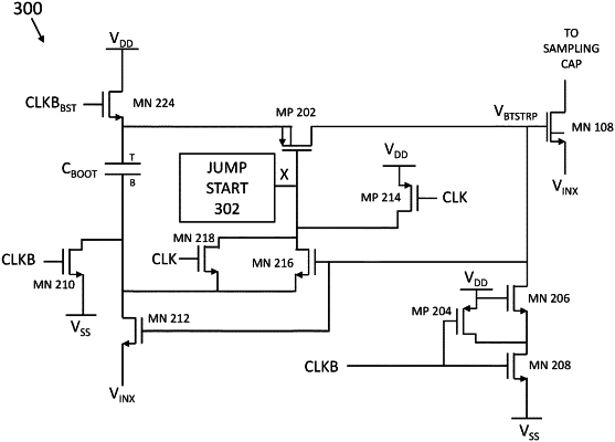
a bootstrapped voltage generator comprising a positive feedback loop, wherein:
the positive feedback loop is activated by a clock signal to generate the gate voltage for turning on the sampling switch; and
the positive feedback loop comprises:
an output transistor to output the gate voltage of the sampling switch;
exactly one capacitor having a first plate and a second plate, wherein the exactly one capacitor is to be charged at the supply voltage in a first phase, and the second plate is coupled to a source of the output transistor; and
an input transistor to receive the voltage input signal and the gate voltage, the input transistor to couple the voltage input signal to the first plate during a second phase; and
a jump start circuit coupled to a gate of the output transistor and configured to turn on the output transistor by decreasing a gate voltage of a gate of the output transistor toward a ground node voltage for a limited period of time during a startup of the positive feedback loop, and to cease the decreasing the gate voltage before the gate voltage reaches the ground node voltage.
|