| CPC H03H 9/0552 (2013.01) [H03B 5/32 (2013.01); H03H 9/1021 (2013.01); H03H 9/19 (2013.01)] | 5 Claims |
|
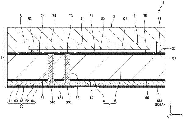
1. A vibrator device comprising:
a vibrator element;
a semiconductor substrate having a first surface on which the vibrator element is disposed and a second surface positioned on an opposite side of the first surface;
a fractional N-PLL circuit disposed at the second surface;
a wiring that is disposed at the first surface and electrically couples the vibrator element and the fractional N-PLL circuit; and
an output terminal that is disposed at the second surface side of the semiconductor substrate, is electrically coupled to the fractional N-PLL circuit, and outputs a signal from the fractional N-PLL circuit, wherein
the output terminal does not overlap the wiring in a plan view along a thickness direction of the semiconductor substrate.
|