| CPC H03H 7/0115 (2013.01) [H01F 27/2804 (2013.01); H01F 27/40 (2013.01); H01G 4/30 (2013.01); H01F 2027/2809 (2013.01); H03H 2001/0085 (2013.01)] | 12 Claims |
|
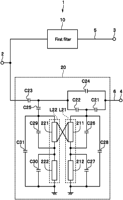
1. A multilayer electronic component comprising:
a stack including a plurality of dielectric layers that are stacked together;
a first inductor integrated with the stack and wound about a first axis orthogonal to a stacking direction of the plurality of dielectric layers;
a second inductor integrated with the stack and wound about a second axis orthogonal to the stacking direction;
a third inductor integrated with the stack and wound about a third axis orthogonal to the stacking direction; and
a fourth inductor integrated with the stack and wound about a fourth axis orthogonal to the stacking direction, wherein
the second inductor is disposed after the first inductor in a first direction orthogonal to the stacking direction,
the third inductor and the fourth inductor are disposed after the first inductor and the second inductor, respectively, in a second direction orthogonal to the stacking direction and the first direction,
the first inductor and the fourth inductor each include a plurality of first through hole columns and at least one first conductor layer portion,
the second inductor and the third inductor each include a plurality of second through hole columns and at least one second conductor layer portion,
the plurality of first through hole columns and the plurality of second through hole columns are each constituted by two or more through holes connected in series to each other,
the at least one first conductor layer portion and the at least one second conductor layer portion each include at least one conductor layer,
two or more of the plurality of first through hole columns are connected in parallel to a part near each end of the at least one first conductor layer portion in a longitudinal direction, and
one of the plurality of second through hole columns is connected to a part near each end of the at least one second conductor layer portion in a longitudinal direction.
|