| CPC H03F 1/08 (2013.01) [H01L 24/13 (2013.01); H01L 27/1022 (2013.01); H01L 29/7371 (2013.01); H03F 3/213 (2013.01); H01L 2224/13025 (2013.01); H01L 2924/13051 (2013.01); H01L 2924/1421 (2013.01); H03F 2200/447 (2013.01); H03F 2200/451 (2013.01)] | 20 Claims |
|
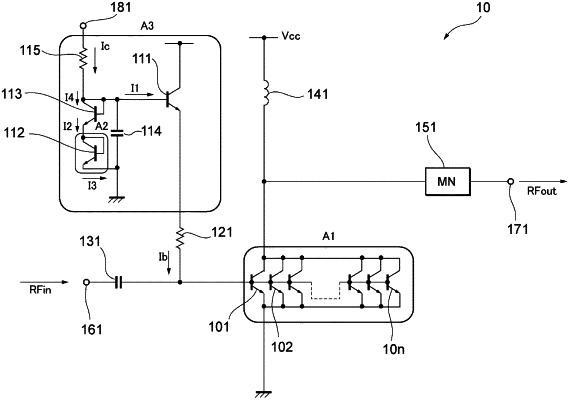
1. A power amplifier circuit comprising:
a first transistor on a semiconductor substrate;
a second transistor on the semiconductor substrate, the second transistor having a base supplied with a first current and being configured to supply a bias current based on the first current to the first transistor;
a current output circuit element on the semiconductor substrate, the current output circuit element being supplied with a second current and being configured to output a third current based on the second current, the second current increasing in accordance with a rise in temperature; and
wiring comprising a plurality of metal layers that are electrically connected to an emitter of the first transistor and that are stacked on top of each other,
wherein the first current and the second current are part of a control current, and
wherein, as seen in a plan view of the semiconductor substrate:
the plurality of metal layers overlap the first transistor and an area between the first transistor and the current output circuit element, and
at least one of the plurality of metal layers further overlaps the current output circuit element.
|