| CPC H02M 3/07 (2013.01) [G11C 5/145 (2013.01); H02M 3/071 (2021.05)] | 20 Claims |
|
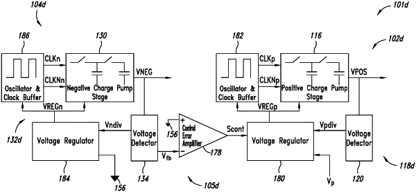
1. A voltage supply circuit, comprising:
a first charge pump stage configured to generate a first voltage having a first polarity;
a second charge pump stage configured to generate a second voltage having a second polarity that is different from the first polarity;
an oscillator configured to output a clock signal to the first charge pump stage;
a regulator configured to supply the oscillator with a regulated voltage; and
a control stage configured to:
receive a voltage representative of a magnitude of the second voltage;
compare the voltage representative of the magnitude of the second voltage with a first reference voltage; and
in response to determining that the magnitude of the second voltage exceeds the first reference voltage, cause the regulator to decrease the regulated voltage.
|