| CPC H02H 7/20 (2013.01) [H01R 13/713 (2013.01); H01R 24/60 (2013.01); H02H 1/0007 (2013.01); H02H 3/20 (2013.01); H01R 2107/00 (2013.01)] | 18 Claims |
|
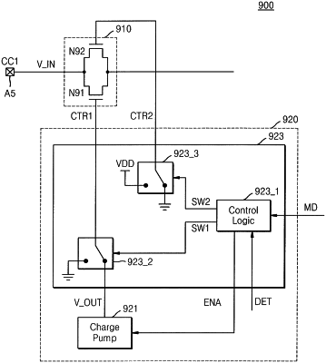
1. A circuit to protect against an overvoltage in a universal serial bus (USB) device that operates in a normal mode and a low-power mode, the circuit comprising:
an overvoltage protection (OVP) switch connected to a pin of a USB receptacle; and
a switch controller configured to detect an overvoltage of the pin and turn off the OVP switch in response to the overvoltage,
wherein the switch controller is configured to provide a first voltage boosted from a second voltage to the OVP switch in the normal mode and to provide the second voltage to the OVP switch in the low-power mode, so that the OVP switch turns on, and
wherein the switch controller is configured to provide a third voltage to the OVP switch in the normal mode and the low-power mode so that the OVP switch turns off,
wherein the OVP switch comprises a first transistor and a second transistor connected in parallel to each other, and
the switch controller is further configured
to provide the first voltage to the first transistor in the normal mode so that the first transistor turns on, and
to provide the third voltage to the first transistor in the low-power mode so that the first transistor turns off.
|