| CPC H01S 5/34333 (2013.01) [H01S 5/021 (2013.01); H01S 5/0206 (2013.01); H01S 5/0213 (2013.01); H01S 5/0215 (2013.01); H01S 5/0216 (2013.01); H01S 5/0217 (2013.01); H01S 5/0218 (2013.01); H01S 5/0234 (2021.01); H01S 5/0425 (2013.01); H01S 5/22 (2013.01); H01S 5/222 (2013.01); H01S 5/2214 (2013.01); H01S 5/32308 (2013.01); H01S 5/04253 (2019.08); H01S 5/04254 (2019.08); H01S 5/2009 (2013.01); H01S 5/2031 (2013.01); H01S 5/30 (2013.01); H01S 2301/173 (2013.01); H01S 2302/00 (2013.01)] | 19 Claims |
|
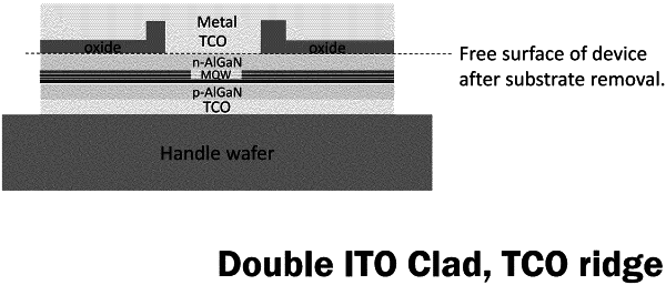
1. An ultraviolet laser diode device operable at a wavelength of less than 380 nm and greater than 200 nm, the ultraviolet laser diode device comprising:
a handle substrate member comprising a surface region;
an interface region overlying the surface region;
a first transparent conductive oxide material with a band gap energy of greater than 3.2 eV and less than 7.5 eV overlying the interface region;
a p-type aluminum, gallium, and nitrogen containing material;
an active region comprising aluminum, gallium, and nitrogen containing material overlying the p-type aluminum, gallium, and nitrogen containing material; and
an n-type aluminum, gallium, and nitrogen containing material;
wherein a process of forming the ultraviolet laser diode device comprises:
bonding the interface region to the surface region; and
subjecting a release material to an energy source to initiate release of the n-type aluminum, gallium, and nitrogen containing material from the release material.
|