| CPC H01S 5/125 (2013.01) [H01S 5/026 (2013.01); H01S 5/0265 (2013.01); H01S 5/1218 (2013.01)] | 12 Claims |
|
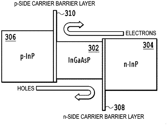
1. A wavelength-tunable DBR laser in which an active region having an optical gain and a DBR region including a diffraction grating are integrated monolithically and an oscillation wavelength is changed by injecting a current into the DBR region, the wavelength-tunable DBR laser comprising:
at a boundary between a p-side clad layer and a core layer in the DBR region, an electron barrier layer being p-type doped and having a bandgap greater than in the p-side clad layer; and
at a boundary between an n-side clad layer and the core layer in the DBR region, a hole barrier layer being n-type doped and having a bandgap greater than in the n-side clad layer.
|