| CPC H01Q 9/0485 (2013.01) [H01Q 1/243 (2013.01); H01Q 3/22 (2013.01); H01Q 9/0407 (2013.01)] | 20 Claims |
|
1. An electronic device comprising:
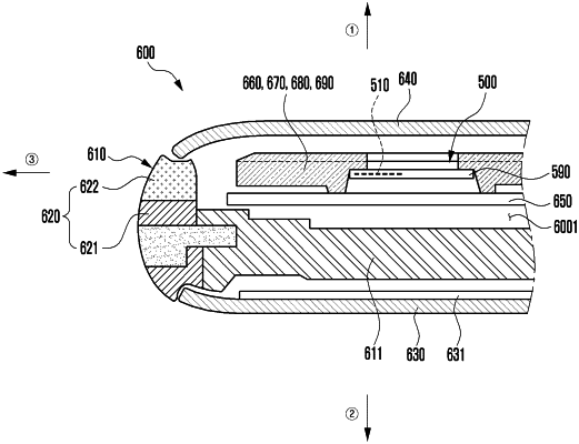
a housing comprising a first cover facing a first direction, a second cover facing a second direction opposite to the first cover and lateral member surrounding an inner space between the first cover and the second cover, and the first cover having a first dielectric constant; and
an antenna structure disposed in the inner space of the housing and comprising:
a printed circuit board (PCB);
at least one antenna element disposed in the PCB to form a beam pattern in a third direction facing the lateral member and being perpendicular to the first direction;
a first dielectric structure disposed on a radiation path of the beam pattern, formed integrally with or combined with the PCB, and having a second dielectric constant, the first dielectric structure being spaced apart from the lateral member;
a second dielectric structure disposed on the radiation path between the first dielectric structure and the first cover, and having a third dielectric constant higher than the first dielectric constant and the second dielectric constant; and
a wireless communication circuit configured to at least one of transmit or receive a radio signal through the at least one antenna element,
wherein at least a part of the second dielectric structure is disposed between the PCB and the lateral member.
|