| CPC H01L 33/405 (2013.01) [H01L 33/06 (2013.01); H01L 33/32 (2013.01); H01L 33/502 (2013.01); H01L 33/58 (2013.01); H01L 33/382 (2013.01); H01L 2933/0016 (2013.01)] | 13 Claims |
|
1. A light emitting diode (LED), comprising:
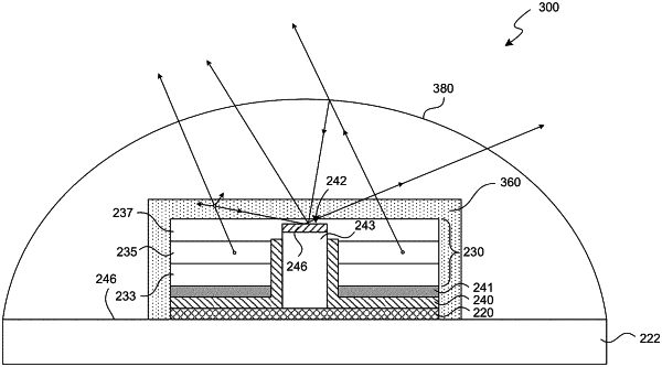
a transduction structure including a back side, a front side opposite the back side, a first semiconductor material having a surface at the back side, a second semiconductor material having a surface at the front side, and a light-emitting active material between the first and second semiconductor materials; and
an electrical connector having—
a base material electrically coupled to the second semiconductor material and including a top side facing the front side of the transduction structure,
a buried contact having the base material extending through the first semiconductor material and the active material from the back side of the transduction structure to a depth in the second semiconductor material such that the base material separates a first portion of the active material from a second portion of the active material, and
a reflective material disposed between the second semiconductor material and at least a portion of the base material nearest the front side of the transduction structure, wherein the reflective material covers at least the top side of the base material.
|