| CPC H01L 33/20 (2013.01) [H01L 33/0093 (2020.05); H01L 33/0095 (2013.01); H01L 33/44 (2013.01); H01L 2933/0025 (2013.01)] | 5 Claims |
|
1. A method for fabricating a flip chip light emitting diode (FCLED) die comprising:
providing a substrate;
providing a plurality of die sized semiconductor structures, each semiconductor structure comprising an epitaxial stack comprising a P-layer, an N-layer, and an active layer between the P-layer and the N-layer configured to emit light, the epitaxial stack having a surface; and one or more metal electrodes on the surface of the epitaxial stack, each metal electrode making electrical contact to the P-layer or the N-layer;
providing a receiving plate comprising an elastomeric polymer layer;
applying an adhesive force to the metal electrodes by placing the metal electrodes in contact with the elastomeric polymer layer with the semiconductor structures still physically connected to the substrate;
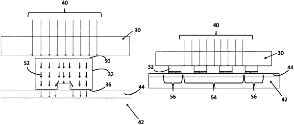
performing a laser lift-off (LLO) process by directing a uniform laser beam through the substrate to the semiconductor layer at an interface of the semiconductor structures with the substrate to lift off the semiconductor structures onto the elastomeric polymer layer; and
removing the semiconductor structures from the receiving plate.
|