| CPC H01L 33/20 (2013.01) [H01L 33/0093 (2020.05); H01L 33/0095 (2013.01); H01L 33/44 (2013.01); H01L 2933/0025 (2013.01)] | 4 Claims |
|
1. A method for fabricating light emitting diode (LED) dice comprising:
providing a plurality of die sized semiconductor structures on a substrate, the semiconductor structures comprised of electrodes and epitaxial stacks of compound semiconductor materials;
providing a receiving plate having a spin coated curable silicone elastomeric polymer layer thereon;
applying an adhesive force to the electrodes by placing the electrodes in contact with the elastomeric polymer layer with the semiconductor structures still physically connected to the substrate;
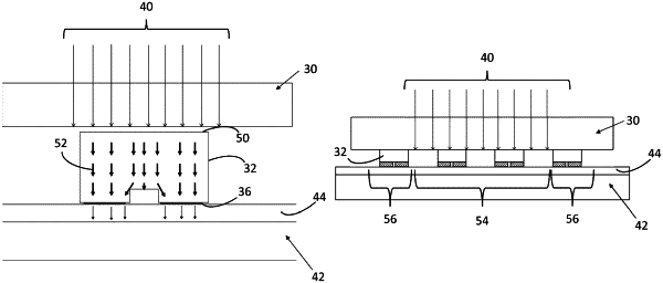
performing a laser lift-off (LLO) process by directing a uniform laser beam through the substrate to the semiconductor layer at an interface with the substrate to lift off the semiconductor structures onto the elastomeric polymer layer, with the elastomeric polymer layer functioning as a shock absorber and an adhesive surface for holding the semiconductor structures; and
selecting a laser wavelength and power such that during the laser lift-off (LLO) process the laser beam can transmit through the substrate and be absorbed by the semiconductor layer at the interface with the substrate.
|