| CPC H01L 33/0012 (2013.01) [H01L 33/06 (2013.01); H01L 33/325 (2013.01); H01L 33/508 (2013.01); H01L 33/60 (2013.01)] | 27 Claims |
|
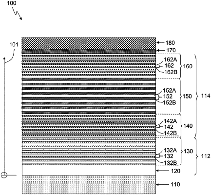
1. A semiconductor structure, comprising:
a first conductivity type region comprising a first superlattice; and
an i-type active region adjacent to the first conductivity type region, the i-type active region comprising an i-type superlattice;
wherein:
the first conductivity type region is a p-type region or an n-type region;
the first superlattice is comprised of a plurality of first unit cells;
the i-type superlattice is comprised of a plurality of i-type unit cells;
each of the plurality of first unit cells comprises a first set of at least two distinct substantially single crystal layers;
each of the plurality of i-type unit cells comprises a second set of at least two distinct substantially single crystal layers;
an average alloy content of the plurality of the first unit cells and the i-type unit cells is constant along a growth direction; and
a combined thickness of the second set of at least two distinct substantially single crystal layers is thicker than a combined thickness of the first set of at least two distinct substantially single crystal layers.
|