| CPC H01L 31/03845 (2013.01) [H01L 27/14643 (2013.01); H01L 27/14679 (2013.01); H01L 31/02161 (2013.01); H01L 31/1126 (2013.01); H01L 31/1136 (2013.01); H01L 31/0336 (2013.01)] | 20 Claims |
|
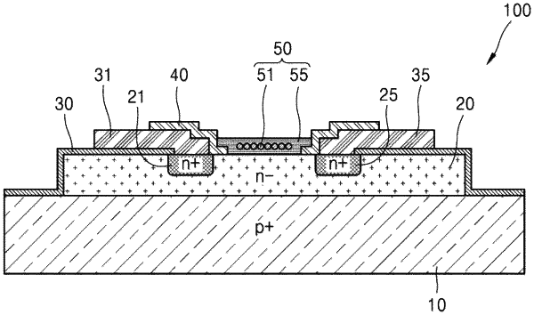
1. An opto-electronic device comprising:
a base portion;
a first electrode provided on an upper surface of the base portion;
a second electrode provided on the upper surface of the base portion and spaced apart from the first electrode;
a quantum dot layer provided between the first electrode and the second electrode on the base portion, the quantum dot layer comprising a plurality of quantum dots; and
a bank structure covering at least a first partial region of the first electrode and at least a second partial region of the second electrode, the bank structure defining a region where the quantum dot layer is formed and comprising an inorganic material,
wherein the first electrode and the second electrode each have a step structure such that a first upper surface thereof is higher than a second upper surface thereof, and
wherein a lateral distance from the first upper surface to the quantum dot layer is greater than a lateral distance from the second upper surface to the quantum dot layer.
|