| CPC H01L 29/78696 (2013.01) [H01L 29/0673 (2013.01); H01L 29/0843 (2013.01); H01L 29/0847 (2013.01); H01L 29/4232 (2013.01); H01L 29/42392 (2013.01); H01L 29/66545 (2013.01); H01L 29/7851 (2013.01); H01L 29/7854 (2013.01)] | 20 Claims |
|
1. A method of manufacturing a semiconductor device, comprising:
forming a stacked structure by alternately stacking sacrificial layers and channel layers on a substrate;
removing a portion of the stacked structure extending in a first direction; forming active regions extending in the first direction by removing a portion of the substrate;
forming sacrificial gate structures extending in a second direction to intersect the active regions, on the substrate;
removing a portion of the stacked structure exposed between the sacrificial gate structures and defining channel structures including the channel layers having a same length to each other in the second direction;
forming source/drain regions on the active regions, on both sides of the sacrificial gate structures;
forming an interlayer insulating layer covering the source/drain regions and filling a gap between the sacrificial gate structures; and
removing the sacrificial gate structures and forming gate structures in regions in which the sacrificial gate structures are removed,
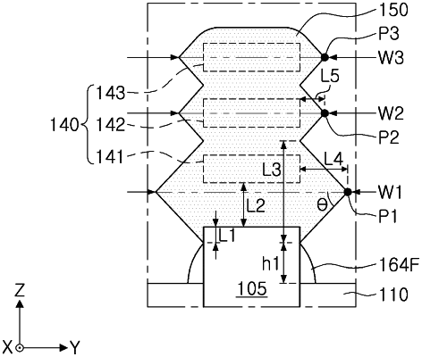
wherein the source/drain regions are grown from sidewalls of the active regions with facets provided along a crystal plane,
the source/drain regions have first protruding points and second protruding points sequentially located from the active regions in a third direction perpendicular to the first and second directions,
the first protruding points protrude further than the second protruding points in the second direction, and
a protruding length of the first protruding points in the second direction is controlled by and is positively correlated with a contact length of the sidewalls of the active regions and the source/drain regions in the third direction.
|