| CPC H01L 29/78675 (2013.01) [H01L 29/0649 (2013.01); H01L 29/42364 (2013.01); H01L 29/42384 (2013.01); H01L 29/4908 (2013.01); H01L 29/66545 (2013.01); H01L 29/66742 (2013.01); H01L 29/66757 (2013.01); H01L 29/66969 (2013.01); H01L 29/7869 (2013.01); H01L 29/78666 (2013.01); H01L 29/78681 (2013.01); H01L 29/78684 (2013.01); H01L 29/78696 (2013.01)] | 20 Claims |
|
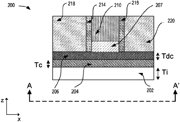
1. A top-gate thin film transistor (TFT) comprising:
a semiconductor layer doped with one or more dopant elements;
a dielectric layer adjacent to the semiconductor layer;
a gate comprising a metal, wherein the gate is adjacent to the dielectric layer;
a spacer adjacent to the gate and the dielectric layer; and
a contact adjacent to the spacer,
wherein the semiconductor layer is doped with the one or more dopant elements beneath each of the dielectric layer, the spacer, and the contact.
|