| CPC H01L 29/78642 (2013.01) [H01L 21/02647 (2013.01); H01L 29/04 (2013.01); H01L 29/0847 (2013.01); H01L 29/1037 (2013.01); H01L 29/42384 (2013.01); H01L 29/6656 (2013.01); H01L 29/6675 (2013.01); H01L 29/78648 (2013.01); H01L 29/78696 (2013.01); H10B 12/05 (2023.02); H10B 12/315 (2023.02); H10B 12/50 (2023.02); H01L 21/31116 (2013.01); H01L 29/66969 (2013.01); H01L 29/7869 (2013.01)] | 20 Claims |
|
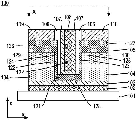
1. A thin film transistor structure, comprising:
a semiconductor layer defining a trench within first and second portions of the semiconductor layer, the first portion over a first gate dielectric layer and the second portion over a sidewall of a patterned layer, wherein the patterned layer is adjacent the first gate dielectric layer;
a first gate electrode opposite the first gate dielectric layer from the first portion of the semiconductor layer;
a second gate electrode at least partially within the trench defined by the semiconductor layer;
a second gate dielectric layer between the second gate electrode and the first portion of the semiconductor layer; and
a source and a drain coupled to the semiconductor layer.
|