| CPC H01L 29/7854 (2013.01) [H01L 21/0217 (2013.01); H01L 21/02247 (2013.01); H01L 21/31053 (2013.01); H01L 21/31111 (2013.01); H01L 21/31144 (2013.01); H01L 29/0649 (2013.01); H01L 29/66818 (2013.01)] | 8 Claims |
|
1. A method for fabricating a fin structure for fin field effect transistor, comprising:
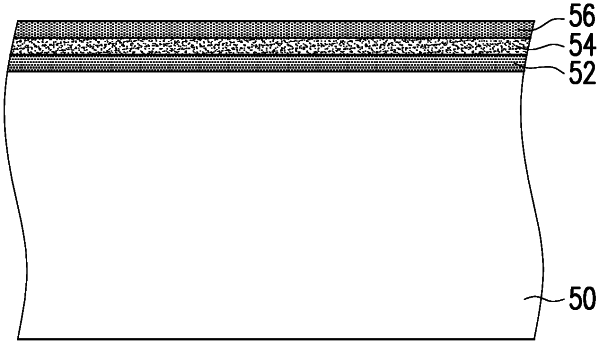
providing a substrate, including a fin structure having a silicon fin and a single mask layer just on a top of the silicon fin, the single mask layer being as a top portion of the fin structure;
forming a stress buffer layer on the substrate and conformally covering over the fin structure;
forming an atomic layer deposition (ALD) layer between the stress buffer layer and each of the silicon fins;
performing a nitridation treatment on the stress buffer layer to have a nitride portion;
perform a flowable deposition process to form a flowable dielectric layer to cover over the fin structures;
annealing the flowable dielectric layer; and
polishing the flowable dielectric layer, wherein the nitride portion of the stress buffer layer is used as a polishing stop.
|