| CPC H01L 29/7839 (2013.01) [H03K 17/6871 (2013.01); H03F 3/245 (2013.01); H03F 2200/451 (2013.01)] | 20 Claims |
|
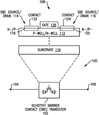
1. A method of fabricating a transistor, the method comprising:
forming a p-well or an n-well in a substrate;
forming a gate for the transistor;
doping a first region within the p-well or the n-well with a concentration that is below a threshold to form a source for the transistor;
doping a second region within the p-well or the n-well with the concentration to form a drain for the transistor, at least a portion of the p-well or the n-well being disposed between the source and the drain of the transistor; and
forming a first contact on the first region and a second contact on the second region.
|