US 11,862,719 B2
Group III-nitride high-electron mobility transistors with buried p-type layers and process for making the same
Saptharishi Sriram, Cary, NC (US); Thomas Smith, Raleigh, NC (US); Alexander Suvorov, Durham, NC (US); and Christer Hallin, Hillsborough, NC (US)
Assigned to Wolfspeed, Inc., Durham, NC (US)
Filed by CREE, INC., Durham, NC (US)
Filed on Dec. 16, 2020, as Appl. No. 17/123,727.
Application 17/123,727 is a division of application No. 16/376,596, filed on Apr. 5, 2019, granted, now 10,892,356.
Application 16/376,596 is a continuation in part of application No. 16/260,095, filed on Jan. 28, 2019, granted, now 10,840,334, issued on Nov. 17, 2020.
Application 16/260,095 is a continuation in part of application No. 15/424,209, filed on Feb. 3, 2017, granted, now 10,192,980, issued on Jan. 29, 2019.
Application 15/424,209 is a continuation in part of application No. 15/192,545, filed on Jun. 24, 2016, granted, now 11,430,882.
Prior Publication US 2021/0104623 A1, Apr. 8, 2021
Int. Cl. H01L 29/778 (2006.01); H01L 29/20 (2006.01); H01L 29/423 (2006.01); H01L 29/66 (2006.01); H01L 29/417 (2006.01); H01L 29/40 (2006.01); H01L 29/10 (2006.01)
CPC H01L 29/7786 (2013.01) [H01L 29/1075 (2013.01); H01L 29/2003 (2013.01); H01L 29/402 (2013.01); H01L 29/41725 (2013.01); H01L 29/42316 (2013.01); H01L 29/66462 (2013.01); H01L 29/7783 (2013.01); H01L 29/7787 (2013.01); H01L 29/1066 (2013.01); H01L 29/41766 (2013.01)] 29 Claims
OG exemplary drawing
 
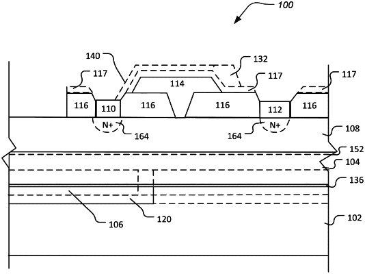
1. An apparatus, comprising:
a substrate;
a group III-Nitride buffer layer on the substrate;
a group III-Nitride barrier layer on the group III-Nitride buffer layer, the group III-Nitride barrier layer comprising a higher bandgap than a bandgap of the group III-Nitride buffer layer;
a source electrically coupled to the group III-Nitride barrier layer;
a gate electrically coupled to the group III-Nitride barrier layer;
a drain electrically coupled to the group III-Nitride barrier layer; and
a p-region being at least one of the following: in the substrate or on the substrate below said group III-Nitride barrier layer,
wherein the p-region is buried below said group III-Nitride barrier layer and the p-region is configured without a p-type material contact and without a connection.