| CPC H01L 29/6681 (2013.01) [H01L 29/0657 (2013.01); H01L 29/16 (2013.01)] | 20 Claims |
|
1. A semiconductor device, comprising:
an isolation insulating layer disposed over a substrate;
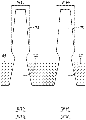
a fin structure having a bottom part and an upper part disposed over the substrate, the upper part protruding the isolation insulating layer;
a gate structure disposed over the upper part of the fin structure;
a source/drain structure, wherein:
the upper part includes a bottom portion and an upper portion disposed on the bottom portion,
the bottom part has a tapered shape and the bottom portion of the upper part has a reverse tapered shape,
a portion having a minimum width of the fin structures, which is located below a portion having a largest width, is covered by a gate dielectric layer,
the gate dielectric layer is in contact with the isolation insulating layer, and
an entirety of the upper part of the fin structure including the bottom portion and the upper portion is made of a same semiconductor material, and is made of a different semiconductor material than the bottom part of the fin structure.
|