| CPC H01L 29/66742 (2013.01) [H01L 21/31116 (2013.01); H01L 21/823418 (2013.01); H01L 29/7869 (2013.01); H01L 29/78633 (2013.01)] | 9 Claims |
|
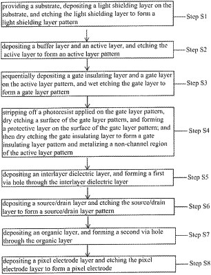
1. A method for fabricating a thin film transistor substrate, comprising:
Step S1: providing a substrate, depositing a light shielding layer on the substrate, and etching the light shielding layer to form a light shielding layer pattern;
Step S2: sequentially depositing a buffer layer and an active layer, and etching the active layer to form an active layer pattern;
Step S3: sequentially depositing a gate insulating layer and a gate layer on the active layer pattern, and wet etching the gate layer to form a gate layer pattern with a photoresist;
Step S4: stripping off the photoresist, and after the photoresist is removed, dry etching a surface of the gate layer pattern by using a fluorine-based etching gas and forming a protective layer on the surface of the gate layer pattern; and dry etching the gate insulating layer to form a gate insulating layer pattern and making conductive a non-channel region of the active layer pattern, wherein an orthographic projection of the gate layer pattern projected on the substrate completely coincides with an orthographic projection of the gate insulating pattern projected on the substrate, and the entire active layer pattern is under the gate insulating layer pattern;
Step S5: depositing an interlayer dielectric layer, and forming a first via hole through the interlayer dielectric layer;
Step S6: depositing a source/drain layer and etching the source/drain layer to form a source/drain layer pattern;
Step S7: depositing an organic layer, and forming a second via hole through the organic layer; and
Step S8: depositing a pixel electrode layer and etching the pixel electrode layer to form a pixel electrode.
|