| CPC H01L 29/66462 (2013.01) [H01L 29/205 (2013.01); H01L 29/4236 (2013.01); H01L 29/42376 (2013.01); H01L 29/7786 (2013.01); H01L 29/7787 (2013.01); H01L 29/2003 (2013.01)] | 15 Claims |
|
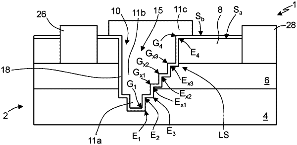
1. A normally off heterostructure field-effect transistor (HEMT), comprising:
a semiconductor heterostructure including:
a first semiconductor layer formed by gallium nitride; and
a second semiconductor layer formed by aluminum gallium nitride;
a passivation layer of dielectric material on the semiconductor heterostructure;
a trench in the passivation layer and the semiconductor heterostructure, the trench including:
a bottom surface;
a planar vertical sidewall in the semiconductor heterostructure on a first side of the trench; and
a plurality of first steps each including a respective horizontal surface higher in the trench than the bottom surface and a respective vertical surface laterally opposite the planar vertical sidewall on a second side of the trench in the semiconductor heterostructure, wherein the planar vertical sidewall extends entirely through the second semiconductor layer.
|