US 11,862,705 B2
Electronic devices and methods of manufacturing the same
Jinseong Heo, Seoul (KR); Yunseong Lee, Osan-si (KR); Taehwan Moon, Suwon-si (KR); and Sanghyun Jo, Seoul (KR)
Assigned to Samsung Electronics Co., Ltd., Gyeonggi-do (KR)
Filed by Samsung Electronics Co., Ltd., Suwon-si (KR)
Filed on Mar. 22, 2021, as Appl. No. 17/208,018.
Claims priority of application No. 10-2020-0035808 (KR), filed on Mar. 24, 2020.
Prior Publication US 2021/0305399 A1, Sep. 30, 2021
Int. Cl. H01L 29/51 (2006.01); H01L 21/28 (2006.01)
CPC H01L 29/516 (2013.01) [H01L 21/28158 (2013.01); H01L 29/40111 (2019.08)] 21 Claims
OG exemplary drawing
 
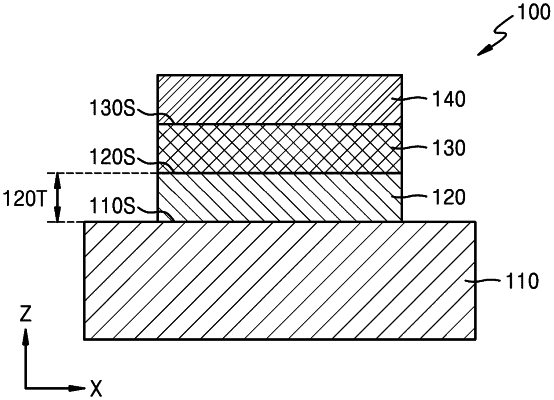
1. An electronic device, comprising:
a substrate;
a seed layer on the substrate, the seed layer including a two-dimensional (2D) material; and
a ferroelectric layer on the seed layer, the ferroelectric layer configured to be aligned within a range of ±30 degrees with respect to a direction in which a (111) crystal direction is perpendicular to a top surface of the substrate,
wherein the seed layer includes a metallic 2D material.