| CPC H01L 29/513 (2013.01) [H01L 21/0228 (2013.01); H01L 21/02115 (2013.01); H01L 21/02164 (2013.01); H01L 21/02178 (2013.01); H01L 21/02181 (2013.01); H01L 21/02189 (2013.01); H01L 21/02356 (2013.01); H01L 29/516 (2013.01)] | 8 Claims |
|
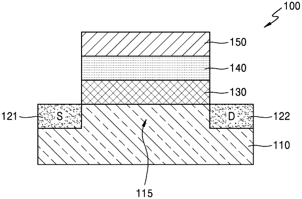
1. A method of manufacturing an electronic device, the method comprising:
preparing a substrate including a channel element;
depositing a carbon layer on the channel element, the carbon layer having an sp2 bonding structure;
depositing a ferroelectric layer on the carbon layer;
depositing a gate electrode on the ferroelectric layer; and
crystallizing the ferroelectric layer through an annealing process.
|