| CPC H01L 29/4236 (2013.01) [H01L 29/401 (2013.01); H01L 29/407 (2013.01); H01L 29/66734 (2013.01); H01L 29/7813 (2013.01)] | 12 Claims |
|
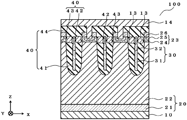
1. A semiconductor device, comprising:
a first electrode;
a second electrode;
a first semiconductor region of a first conductive type provided between the first electrode and the second electrode and electrically connected to the first electrode;
a plurality of second semiconductor regions of a second conductive type provided between the first semiconductor region and the second electrode;
a third semiconductor region of the first conductive type provided between the second semiconductor region and the second electrode and electrically connected to the second electrode;
a conductive portion provided between the first electrode and the second electrode, the conductive portion including a first conductive portion and a second conductive portion, the first conductive portion provided on a side of the conductive portion facing the first electrode in a first direction from the first electrode to the first semiconductor region, the second conductive portion provided on a side of the conductive portion facing the second electrode in the first direction, the second conductive portion disposed between the second semiconductor regions in a second direction crossing the first direction, and the second conductive portion having an impurity concentration lower than an impurity concentration of the first conductive portion;
a first insulating portion provided between the first conductive portion and the first semiconductor region;
a gate electrode provided between the second semiconductor region and the second conductive portion in the second direction;
a second insulating portion provided between the second conductive portion and the gate electrode; and
a third insulating portion provided between the second semiconductor region and the gate electrode.
|